
Answer in brief
Researchers report wafer-scale growth and encouraging transistor tests. The advance addresses a materials bottleneck, while factory integration is still an open question.
The advance is making more of the material
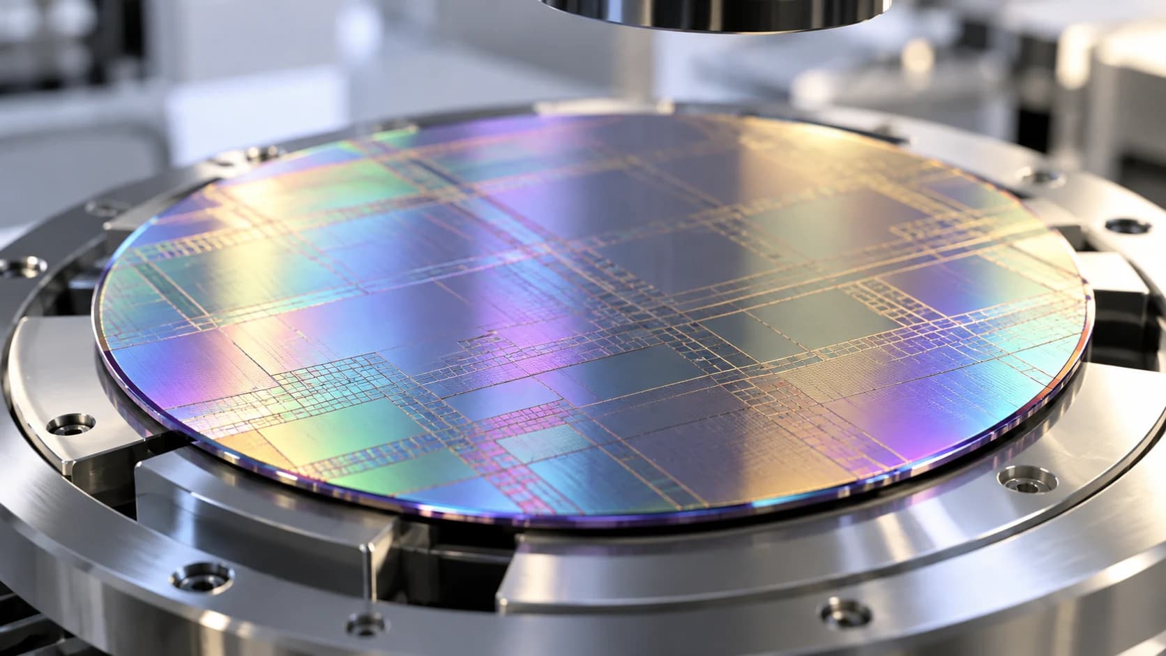
A paper published in Nature Nanotechnology on 29 September reports repeatable four-inch wafers of rhombohedral boron nitride, a layered material with switchable electrical polarization. The researchers used a stepped sapphire template and nickel-boron films to guide crystal growth. Their claim is significant because attractive properties in a tiny flake are of limited manufacturing value if the material cannot be made consistently over a larger area. The paper reports structural checks across batches, but its wafers remain research samples rather than qualified commercial substrates.
What the prototype devices showed
The team built ferroelectric field-effect transistors and arrays using the material. It reports switching on a nanosecond timescale, resistance to more than two billion switching cycles, and an on/off ratio of one million in arrays. Those numbers describe specified laboratory tests under the study's conditions. They should not be read as a promise that a complete memory chip will deliver the same performance after packaging, long-term operation and manufacturing variation. The paper also reports thermal stability and device behaviour at short channel lengths, which invites further replication.
How it relates to earlier work
MIT reported in 2024 on transistors using the sliding-ferroelectric behaviour of stacked boron nitride layers. That earlier account helps explain why researchers are interested: relative layer movement can change a polarization state that persists without continuous power. The new paper tackles a different obstacle, controlled growth of larger single-crystal material and device arrays. It does not invent the basic memory concept or replace all established silicon memory. Its manufacturing relevance will depend on integrating the material with existing fabrication steps at acceptable yield and cost.
The gap from wafer to product
A four-inch demonstration is evidence of scale beyond isolated flakes, but commercial lines also need defect control, uniform device performance, transfer or direct integration, reliable endurance under realistic conditions and a cost case. The study's authors present a potential platform, not a production announcement. At the 30 September evidence cutoff, the strongest supported statement is that a materials-growth hurdle and prototype functionality have been demonstrated in the published experiments. Independent reproduction and process integration will decide whether this becomes a practical nonvolatile memory option.
Questions and answers
Is this boron nitride memory available in chips now?
The paper presents research wafers and prototype transistors and arrays. It does not establish a commercial fabrication process, product qualification or market launch.
What does sliding ferroelectric mean?
A small relative shift between atomically thin layers can switch an electrical polarization state that may store information even after power is removed.